info@amethystresearch.net
Services

We specialize in
FULLY CUSTOMIZED INFRARED SOLUTIONS, starting with
epitaxial structure design and ending with device prototyping
and small-volume manufacturing.
Because, like you, we have commercialization in mind, we
choose solutions that combine ultra-high performance,
cost-effectiveness, and fast development-to-prototype cycle
times.
Whether you are developing a DoD mission-critical system (or
managing sensor innovation for your agency), looking for a
cutting-edge device for your commercial infrared system, or
looking to transfer your ideas out of your research
institution’s lab, we welcome an opportunity to support your
needs.


Custom Design and Fabrication of
Infrared Photodetectors and
Emitters
Device Design/IP
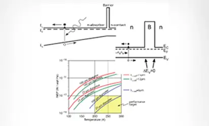
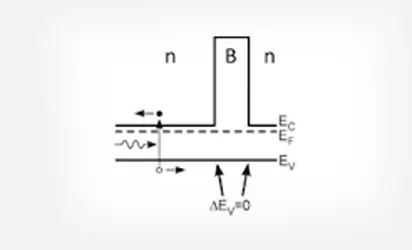
Based on your specifications, such as wavelength range, sensitivity, response time, & the application, our team proposes a detector design (RCE-PDs, APDs, nBn, LEDs or other) & semiconductor materials of choice for the substrate & III-V epilayers.
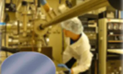
Semiconductor Growth
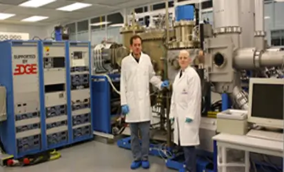
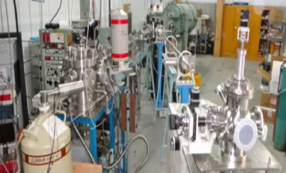
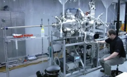
After the design is established, we grow the III-V epitaxial layers using Molecular Beam Epitaxy (Riber R&D reactor).
Materials Characterization
Growth is followed by materials analysis to ensure the quality of the III-V layers prior to the fabrication of the device.
Passivation Technologies
Our proprietary hydrogenation process, undertaken post-growth, improves the epi-wafer quality further by reducing the number of defects that impact electronic properties.
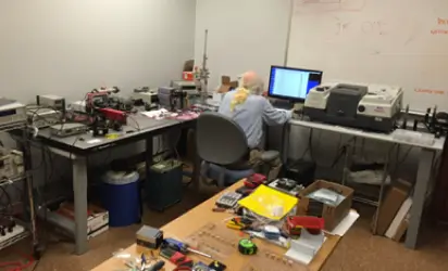
Fabrication & Evaluation
With access to a microelectronics center, we use microfabrication techniques (lithography, etching, doping and contact formation) to make arrays of trial devices. We examine the devices (optical, SEM) and test their opto-electronic properties in an environment suitable for the stage of development.
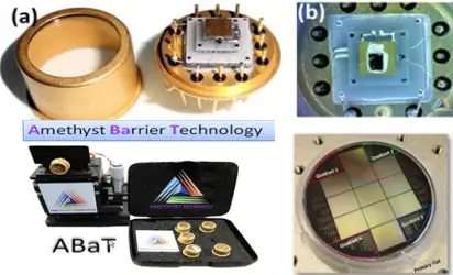
Prototype Packaging
We integrate the prototype devices into standard packages in an inert environment and optionally with a thermoelectric cooler. Typically, we include a trans-impedance amplifier that converts photocurrent to voltage.
Technology Readiness Levels (TRL) from 1 through 6 are addressed entirely with internal capabilities and our established supply chain. Higher TRL’s can be addressed with integration partners.
How Our Capabilities Tie Together
Device Design
Based on your requirements, (wavelength range, sensitivity, response time and other), and selected application, we formulate a detector design within the suite of detector types we develop internally or with our university partners. We have extensive experience in nBn, RCE-PD, APD, SPAD, LED architectures and more.
MBE Growth Of III-V Epilayers
Our focus is on quality. We ensure the best performance and operability of our III-V photodetectors and photoemitters by using our Riber research MBE reactor in conjunction with our proprietary hydrogen passivation process, a technique particularly well suited for compound semiconductors. The scale and flexibility of our MBE growth allows affordability (i.e. for Phase 1 exploratory work). Our specialty is antimonides, arsenides, and dilute phosphides and nitrides.
Materials Characterization
Materials characterization techniques include FTIR-based optical reflection and transmission, Hall Effect, XPS, RBS, NRA, ERDA, PIXE, AFM, XRD and RAMAN. These tools are used to support MBE but can also be used for wafers or materials provided by clients/research partners.Ion beam methods are especially useful for studying point defects and hydrogen incorporation to mitigate defects.
Prototyping
Excellent university-based microelectronics facilities (UT-Austin and Lancaster University) support the fabrication of devices ranging from 25 to 1,000 microns in size and covering the suite of detector types and materials families. Evaluation includes microscopies, spectral response, dark current analysis, sensitivity, detectivity, and quantum efficiency. Packaging processes comprise dicing, thermal bonding, wire-bonding, and sealing. Wavelength and operating temperature determine the materials used.